
Semiconductor & Display
From front-end sputtering to the final wire bond — purity engineered for every layer.
Market trends
Faster, smaller, more precise
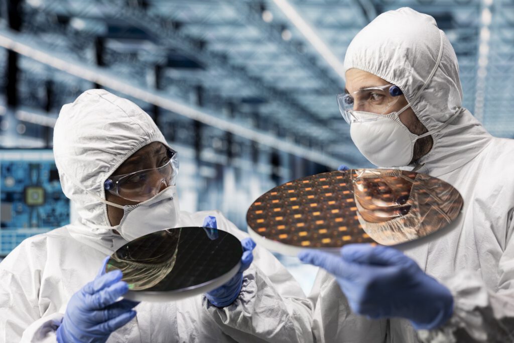
The spread of AI has brought semiconductors to an unprecedented inflection point. As AI compute demand grows explosively, both memory and logic are moving toward higher density and higher performance. 3D stacking and heterogeneous integration have become central to next-generation competitiveness. With them, the precision and quality standards demanded of materials at every process step keep rising.
The display industry is under the same pressure. As OLED goes flexible and micro LED enters commercial production, demands on the purity and uniformity of deposition and electrode materials continue to grow. These shifts are not confined to one region. Advanced manufacturers across Asia, Europe, and the Americas face the same challenge, and LT Metal supports their manufacturing competitiveness with precious metal materials technology and deep process know-how.
Demand by process
Precious metal materials by process step
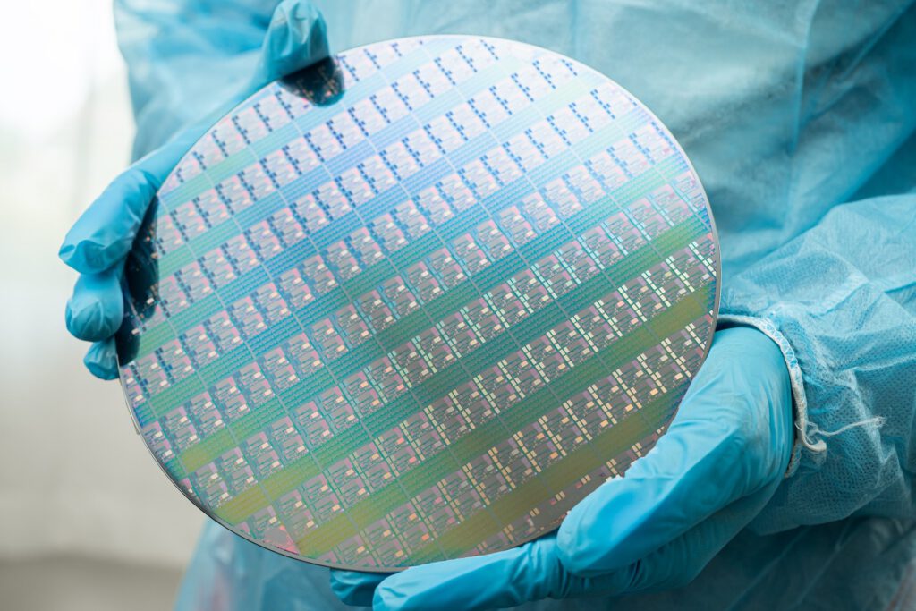
Semiconductor and display manufacturing draws on a wide range of precious metal materials. As technology advances, purity, uniformity, and electrical properties increasingly determine device performance, yield, and reliability.
| Segment | Process step | Materials used | Key requirements | LT Metal products |
|---|---|---|---|---|
| Semiconductor | Front-end — sputtering targets | Au, Ag, Pt, Pd, Ru | 6N (99.9999%) or higher purity; uniform grain structure | Precious metal sputtering targets |
| Front-end — diffusion barrier layer | Ru, Pt | High-temperature oxidation resistance; thin film uniformity | Ru/Pt deposition targets | |
| 3D stacking — TSV plating | Au, precious metal seed layers | Low resistance; void-free fill | Precious metal plating materials and chemicals | |
| Microbump bonding | Au, Ni, Cu, Sn, SnAg | Flip-chip joint reliability | Precious metal solder materials | |
| Wire bonding | Au, Ag, AuPdCu | Loop formability; long-term reliability | Bonding wire | |
| EMI-shield coating | Cu, SUS | EMI shielding; high reliability; uniform thin film | EMI shielding targets | |
| Package terminal plating | Au, Pd-Ni, Ag | Stable contact resistance; corrosion resistance | Selective precious metal plating materials | |
| Display | OLED electrode deposition | Ag, Ni, Cu, Mo, Al, IGZO, ITO, IZO | Transmittance; reflectance; sheet resistance; etch characteristics | Deposition targets for OLED |
| Display interconnect materials | Ag, Ni, Cu, Mo, Al, IGZO, ITO, IZO | Transmittance; reflectance; sheet resistance; etch characteristics | Precious metal materials for thin film interconnects |
Material transitions
Material transitions in the advanced packaging era
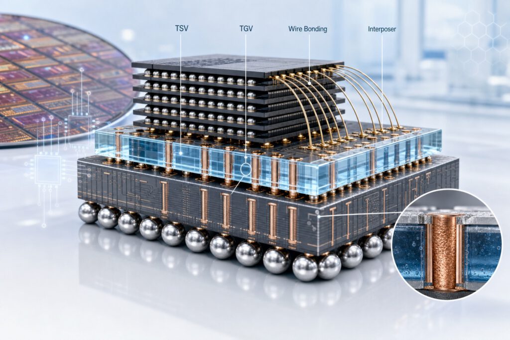
AI accelerators and high-performance computing (HPC) are driving rapid progress in 3D stacked memory. As TSV (Through Silicon Via) density rises, plating uniformity and fill quality become decisive for device performance and yield. LT Metal answers these tightening process requirements with precision precious metal materials technology.
In wire bonding, palladium-coated copper (PCC) wire is displacing gold (Au) wire across a widening range of applications. LT Metal supplies both the material and the process engineering support needed to secure cost competitiveness and reliability together. As flexible and foldable displays and micro LED advance, precious metal joining and electrode materials face new performance standards. LT Metal partners on these material transitions from the development stage onward. We engineer essential materials for tomorrow.
Cases
Applications
Development support for TSV plating materials in high-density 3D memory volume production
High-purity precious metal targets for next-generation OLED panel deposition
Engineering support for the Au → PCC wire transition in semiconductor packaging
Pt/Ir sputtering targets for MEMS sensor electrode processes
Why LT Metal
Three engineering capabilities
Global customers choose LT Metal because our engineering capability in composition, structure, and reliability delivers the performance and quality they specify. That is our core strength.

We engineer composition.
The same precious metal behaves very differently depending on purity and alloying elements: conductivity, heat resistance, and thin film stress all shift. LT Metal analyzes the electrical, thermal, and mechanical demands of your semiconductor or display process, then engineers an alloy composition — down to purity grade and grain size — matched to your process conditions.
We engineer structure.
Composition alone does not make an essential material. Drawing on in-house powder synthesis for functional target materials including ITO targets, we engineer particle size distribution, sintered density, and crystal structure from the start. We also optimize structure to minimize particle generation and arcing, supporting stable process operation.
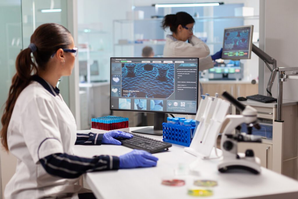
We engineer reliability.
Essential materials must work, every time. Our reliability verification system is built on 6N (99.9999%) purity certification, lot-level Certificates of Conformance (CoC), and XRF and ICP composition analysis that meet the strict quality standards of semiconductor manufacturing.

Start with LT Metal.
We engineer essential materials for tomorrow.
Your next challenge is our next design.
The precious metal material you choose determines your product’s performance and reliability. LT Metal works alongside you across the entire journey — material selection, joint development, volume supply, and recovery after use. Because a single material can move your product one step forward, LT Metal is already engineering the century ahead.
- Technical consultation — material selection, specification review, process compatibility assessment
- Request a sample — small-lot prototyping and evaluation support
- Precious metal recovery — assessment of precious metal content and recovery from spent materials
- Partnership proposal — long-term supply agreements, joint development projects